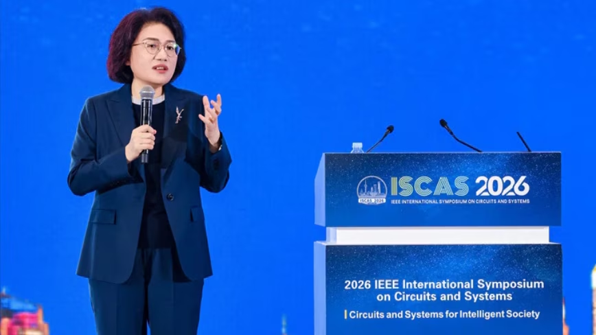
He Tingbo used a Shanghai keynote to argue that cutting signal-propagation time, not shrinking transistors, is the new frontier, and that Huawei has been quietly building chips around the idea for six years.
Huawei used the opening day of the IEEE International Symposium on Circuits and Systems in Shanghai on Monday to argue that the global semiconductor industry needs a different organising principle, and that it has one ready.
He Tingbo, who runs Huawei's semiconductor business and chairs its Scientist Committee, told the conference the company has spent the past six years developing what it calls the Tau (τ) Scaling Law, and is now applying it across its chip line.
The proposition is that geometric scaling, the steady shrinking of transistors that has guided the industry for more than fifty years, is no longer doing the work it used to.
The τ Scaling Law puts the time it takes for signals and data to move through a chip and its surrounding system at the centre of design instead, according to the company's announcement.

The 💜 of EU tech
The latest rumblings from the EU tech scene, a story from our wise ol' founder Boris, and some questionable AI art. It's free, every week, in your inbox. Sign up now!
Shorten that time, the argument runs, and you can keep pushing performance and effective transistor density without depending on the manufacturing breakthroughs Huawei has been cut off from.
He used the keynote, titled “New Semiconductor Path in Practice”, to introduce an architecture called LogicFolding, which Huawei said reorganises circuit layouts to shorten critical-path wiring and reduce the resistive and capacitive load on signal propagation.
The Kirin chips scheduled for launch in the autumn will be the first to ship with it, the company said.
The headline figure is a longer-dated one. By 2031, Huawei expects to design high-end chips with transistor density equivalent to a 1.4-nanometre process, a band most of the industry expects to reach toward the end of the decade through extreme ultraviolet lithography that Chinese firms cannot legally buy.
Huawei did not publish independent performance data to support the projection.
Over the past six years, He said, Huawei has designed and mass-produced 381 chips based on the τ principle, for use in smartphones, AI computing, and other categories the company did not itemise. The claim is, for now, Huawei's alone; no third party has audited the figure.
The backdrop is familiar. Washington has spent four years tightening export controls on the lithography tools, design software, and high-bandwidth memory that the most advanced nodes require, and ASML, the Dutch firm that makes the EUV systems Huawei would need to manufacture at 1.4 nm conventionally, remains barred from shipping its most capable equipment to China.
The MATCH Act under discussion in Washington would tighten the perimeter further. Huawei has responded by trying to design around the constraint rather than wait for it to lift.
The company has been laying the groundwork for that argument in public for months. The tour of its secret chip lab on Chinese state television in late October, two days before Donald Trump's arrival in Beijing, made the point geopolitically. Monday's keynote made it technically. He Tingbo, sometimes referred to in the Chinese press as the country's “chip queen”, has been running Huawei's semiconductor effort since 2003 and is now the public face of the self-reliance push.
Whether the τ Scaling Law is a coherent design philosophy or a rebrand of well-established techniques in circuit-level optimisation will take longer to settle.
The company framed the announcement as an invitation, with He calling for scientists, engineers, and industry partners around the world to work on it jointly.
The audience for that invitation, in practical terms, sits mostly inside China.
The first test will arrive in the autumn, when the Kirin chips reach buyers. The longer one runs to 2031.